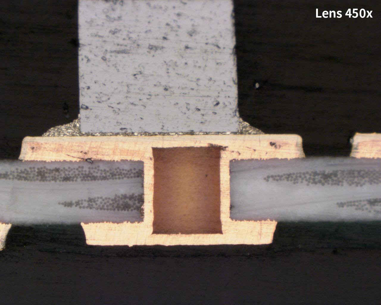
We are able to form component pads (for mounting a component) just above a through-hole by filling a through-hole with resin to make the PWB surface flat.
The “VIA on VIA” structure is formed by applying this technique to the inner layer of a build-up PWB.
Choose epoxy type resin or conductive paste as the hole-plugging material.
Principal use
Multi-chip modules, build-up PWBs, and more