High Density Advanced Fine Pattern and Flip-chip Mounting PCB for Semiconductor Packages.
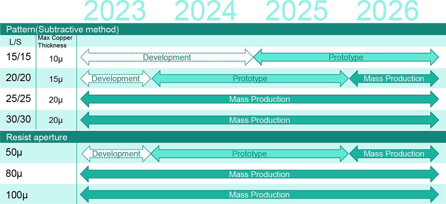
High-density advanced semiconductor packages are used in 5G/mobile communication equipment/server/FC-BGA. We enable us to produce low cost fine patterning by our own subtractive method technology. We add a direct imaging exposure system to the existing contact exposure system, it makes the pattern more high-density and high accuracy.
Design Rules
| Fine 1(Direct imaging) | Fine 2(Contact exposure) | Standard | |
|---|---|---|---|
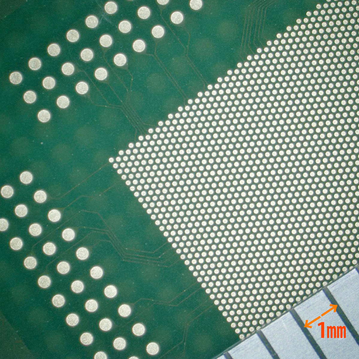
| Pattern position accuracy(to through hole) | ±10μ | ±35μ | ±50μ |
| Solder resist position accuracy (to pattern) | ±30μ | ±50μ | ±75μ |
Technology Roadmap